
How does a transistor work?
Asked by: Tony WhelanAnswer
The design of a transistor allows it to function as an amplifier or a switch. This is accomplished by using a small amount of electricity to control a gate on a much larger supply of electricity, much like turning a valve to control a supply of water.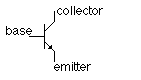 Transistors are composed of three parts ' a base, a collector, and an emitter. The base
is the gate controller device for the larger electrical supply. The collector is the
larger electrical supply, and the emitter is the outlet for that supply. By sending
varying levels of current from the base, the amount of current flowing through the gate
from the collector may be regulated. In this way, a very small amount of current may be
used to control a large amount of current, as in an amplifier. The same process is used to
create the binary code for the digital processors but in this case a voltage threshold of
five volts is needed to open the collector gate. In this way, the transistor is being
used as a switch with a binary function: five volts ' ON, less than five volts ' OFF.
Transistors are composed of three parts ' a base, a collector, and an emitter. The base
is the gate controller device for the larger electrical supply. The collector is the
larger electrical supply, and the emitter is the outlet for that supply. By sending
varying levels of current from the base, the amount of current flowing through the gate
from the collector may be regulated. In this way, a very small amount of current may be
used to control a large amount of current, as in an amplifier. The same process is used to
create the binary code for the digital processors but in this case a voltage threshold of
five volts is needed to open the collector gate. In this way, the transistor is being
used as a switch with a binary function: five volts ' ON, less than five volts ' OFF.
 Semi-conductive materials are what make the transistor possible. Most people are familiar
with electrically conductive and non-conductive materials. Metals are typically thought
of as being conductive. Materials such as wood, plastics, glass and ceramics are
non-conductive, or insulators. In the late 1940's a team of scientists working at Bell
Labs in New Jersey, discovered how to take certain types of crystals and use them as
electronic control devices by exploiting their semi-conductive properties.Most
non-metallic crystalline structures would typically be considered insulators. But by
forcing crystals of germanium or silicon to grow with impurities such as boron or
phosphorus, the crystals gain entirely different electrical conductive properties. By
sandwiching this material between two conductive plates (the emitter and the collector), a
transistor is made. By applying current to the semi-conductive material (base), electrons
gather until an effectual conduit is formed allowing electricity to pass
The scientists that were responsible for the invention of the transistor were John
Bardeen, Walter Brattain, and William Shockley. Their Patent was called: 'Three
Electrode Circuit Element Utilizing Semiconductive Materials.'
Semi-conductive materials are what make the transistor possible. Most people are familiar
with electrically conductive and non-conductive materials. Metals are typically thought
of as being conductive. Materials such as wood, plastics, glass and ceramics are
non-conductive, or insulators. In the late 1940's a team of scientists working at Bell
Labs in New Jersey, discovered how to take certain types of crystals and use them as
electronic control devices by exploiting their semi-conductive properties.Most
non-metallic crystalline structures would typically be considered insulators. But by
forcing crystals of germanium or silicon to grow with impurities such as boron or
phosphorus, the crystals gain entirely different electrical conductive properties. By
sandwiching this material between two conductive plates (the emitter and the collector), a
transistor is made. By applying current to the semi-conductive material (base), electrons
gather until an effectual conduit is formed allowing electricity to pass
The scientists that were responsible for the invention of the transistor were John
Bardeen, Walter Brattain, and William Shockley. Their Patent was called: 'Three
Electrode Circuit Element Utilizing Semiconductive Materials.'
Reference:
Answered by: Stephen Portz, Technology Teacher, Space Coast Middle School, FL
There are two main types of transistors-junction transistors and field effect transistors. Each works in a different way. But the usefulness of any transistor comes from its ability to control a strong current with a weak voltage. For example, transistors in a public address system amplify (strengthen) the weak voltage produced when a person speaks into a microphone. The electricity coming from the transistors is strong enough to operate a loudspeaker, which produces sounds much louder than the person's voice.
JUNCTION TRANSISTORS
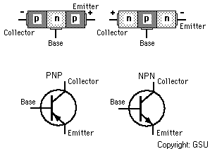 A junction transistor consists of a thin piece of one type of
semiconductor material between two thicker layers of the opposite type. For example, if
the middle layer is p-type, the outside layers must be n-type. Such a transistor is an
NPN transistor. One of the outside layers is called the emitter, and the other is known
as the collector. The middle layer is the base. The places where the emitter joins the
base and the base joins the collector are called junctions.
A junction transistor consists of a thin piece of one type of
semiconductor material between two thicker layers of the opposite type. For example, if
the middle layer is p-type, the outside layers must be n-type. Such a transistor is an
NPN transistor. One of the outside layers is called the emitter, and the other is known
as the collector. The middle layer is the base. The places where the emitter joins the
base and the base joins the collector are called junctions.
The layers of an NPN transistor must have the proper voltage connected across them. The voltage of the base must be more positive than that of the emitter. The voltage of the collector, in turn, must be more positive than that of the base. The voltages are supplied by a battery or some other source of direct current. The emitter supplies electrons. The base pulls these electrons from the emitter because it has a more positive voltage than does the emitter. This movement of electrons creates a flow of electricity through the transistor.
The current passes from the emitter to the collector through the base. Changes in the voltage connected to the base modify the flow of the current by changing the number of electrons in the base. In this way, small changes in the base voltage can cause large changes in the current flowing out of the collector.
Manufacturers also make PNP junction transistors. In these devices, the emitter and collector are both a p-type semiconductor material and the base is n-type. A PNP junction transistor works on the same principle as an NPN transistor. But it differs in one respect. The main flow of current in a PNP transistor is controlled by altering the number of holes rather than the number of electrons in the base. Also, this type of transistor works properly only if the negative and positive connections to it are the reverse of those of the NPN transistor.
FIELD EFFECT TRANSISTORS
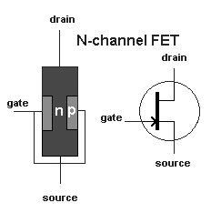 A field effect transistor has only two layers of semiconductor
material, one on top of the other. Electricity flows through one of the layers, called
the channel. A voltage connected to the other layer, called the gate, interferes with the
current flowing in the channel. Thus, the voltage connected to the gate controls the
strength of the current in the channel. There are two basic varieties of field effect
transistors-the junction field effect transistor(JFET) and the metal oxide semiconductor
field effect transistor (MOSFET). Most of the transistors contained in today's
integrated circuits are MOSFETS's.
A field effect transistor has only two layers of semiconductor
material, one on top of the other. Electricity flows through one of the layers, called
the channel. A voltage connected to the other layer, called the gate, interferes with the
current flowing in the channel. Thus, the voltage connected to the gate controls the
strength of the current in the channel. There are two basic varieties of field effect
transistors-the junction field effect transistor(JFET) and the metal oxide semiconductor
field effect transistor (MOSFET). Most of the transistors contained in today's
integrated circuits are MOSFETS's.
Answered by: Justin Shores, High School Student